
EUV lithography optics
Six-mirror EUV projection objective: aperture on the ring field, image quality and light budget
Four-times reduction, image-side NA 0.25, 13.4 nm, six aspheric mirrors after patent US 6,188,513
Six-mirror EUV projection objective: aperture on the ring
field, image quality and light budget
Four-times reduction, image-side NA 0.25, 13.4 nm, six aspheric mirrors after patent US 6,188,513
| The design problem | How the system is modelled |
| Extreme-ultraviolet lithography prints chip patterns with | The starting design is the first embodiment of patent US |
| light of 13.4 to 13.5 nm. No glass transmits there, so the | 6,188,513 [1]. The lens design software etendue offers it |
projection objective uses mirrors alone, each coated with as a starting point for a four-times reduction at NA 0.25
| a Mo/Si multilayer that reflects about 73 % near normal | with a ring field. Each mirror is an off-axis segment of an |
| incidence. To keep the mirrors out of one another's | even asphere. Three field points sit across the ring, 116 to |
| beams, the image is formed on an off-axis ring and the | 124 mm from the axis on the mask. Real rays traced to |
| axis receives no light. A designer has to check that the | the rim of the pupil give the half-angle u of the cone that |
| aperture where the image is formed is the one required, | reaches each point, and its working f-number N = 1/(2 |
| that the image is diffraction-limited across the ring, and | sin u), along the ring radius (tangential) and across it |
| that enough light reaches the wafer. A standard lens | (sagittal). The 40-bilayer Mo/Si coating is computed from |
| design report gives the f-number on axis, where this | the optical constants of Henke et al. [2] at the real angle |
| objective forms no image, and treats mirror coatings as | of every ray. |
perfect.
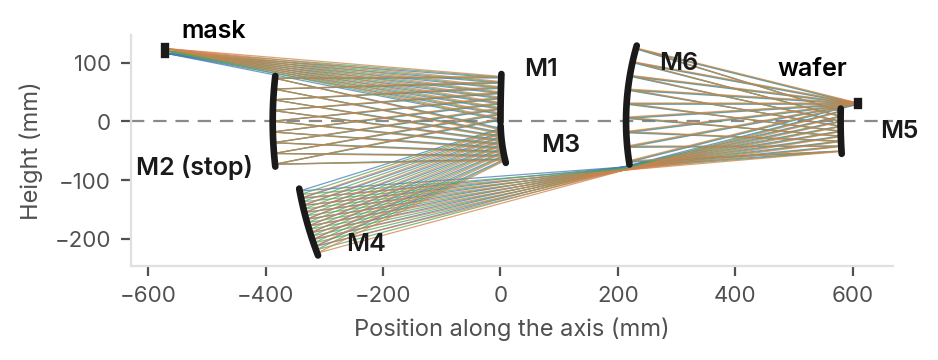
Figure 1. Meridional section, rays traced in etendue. Light from the mask reflects on M1 to M6 in turn and reaches the wafer 30 mm from the axis. Blue, green and orange: rays from 116, 120 and 124 mm on the mask. Dashed line: the optical axis.
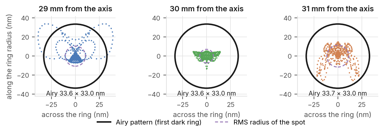
What the analysis shows on the starting design The f-number cannot be measured on axis, since no ray reaches it. At the outer edge of the ring, the working f-number is 2.06 along the ring radius and 2.02 across it, so the Airy pattern (radius 1.22 λN) is an ellipse, 33.7 nm in radius along the ring and 33.0 nm across it. At the three field points the RMS spot radius is 7 to 11 nm, a third of the Airy radius or less, and the RMS wavefront error reaches 0.033 wave at most, below the 0.071 wave of the Maréchal criterion for a diffraction- limited image [5].
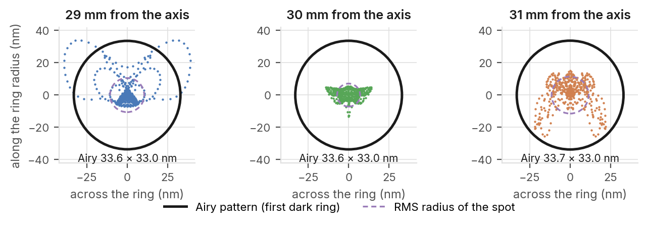
Figure 2. Spot diagrams on the wafer at the three field points, computed in etendue. Black: the Airy pattern at the working f-number of each point. Red dashes: the RMS radius of the spot.
etendue.io 13.4 nm · 4× reduction · NA 0.25 · six mirrors · etendue, October 2026
Light budget of the six coated mirrors
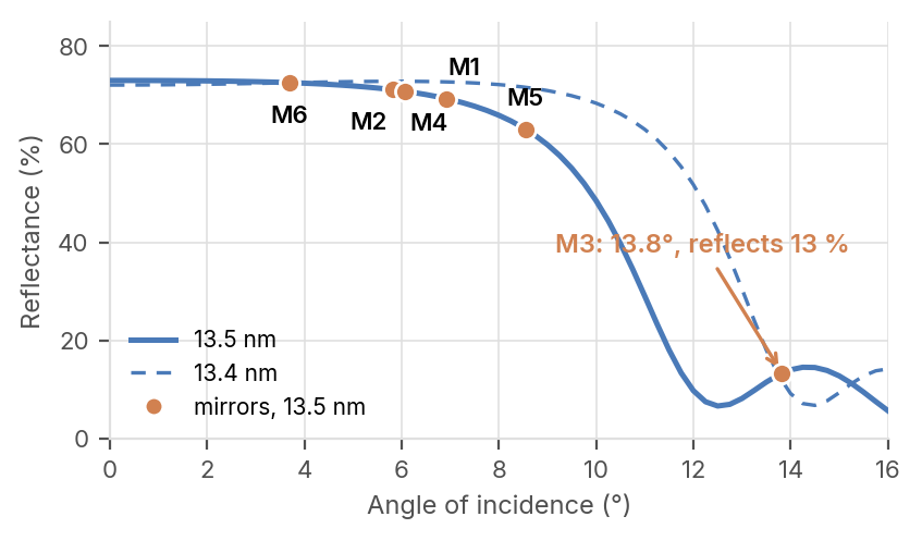
Near normal incidence the Mo/Si stack reflects 73 % at 13.5 nm, and six mirrors at normal incidence would pass 15 % of the light. The same stack coats all six mirrors. Its period is fixed and tuned for incidence close to normal, and beyond about 10° its reflection band moves away from 13.5 nm. The chief ray meets the third mirror at 13.8°, where the stack reflects 13 %, and the fifth at 8.5°, where it reflects 63 %. Along the chief ray at the ring centre the six mirrors pass 2.1 % of the light at 13.5 nm. Averaged over all rays of the pupil, which meet the mirrors at other angles,
| Figure 3. Reflectance of the Mo/Si stack against angle of incidence, | they pass 1.4 % at 13.5 nm and 2.0 % at 13.4 nm, |
| computed in etendue at 13.5 nm (solid) and 13.4 nm (dashed). Dots: each | where the band of the stack reaches slightly larger |
| ^(m)^(i)^(r)^(r)^(o)^(r)^(a)^(t)^(t)^(h)^(e)^(a)^(n)^(g)^(l)^(e)^(o)^(f)^(t)^(h)^(e)^(c)^(h)^(i)^(e)^(f)^(r)^(a)^(y)^(a)^(t)^(t)^(h)^(e)^(r)^(i)^(n)^(g)^(c)^(e)^(n)^(t)^(r)^(e)^(.) | angles (dashed curve). The patent names the first, |
third and fifth mirrors as candidates for graded multilayer coatings [1].
Fidelity to the published design
The RMS wavefront error at five field points is 0.020 to 0.033 wave in the model, against 0.019 to 0.034 wave in the patent [1]. The largest distortion on the ring is 2.06 nm, against 2.07 nm. Computed point by point across the field, the RMS wavefront error stays below the Maréchal criterion from 28.6 to 31.3 mm from the axis on the wafer, a band 2.7 mm wide; the patent uses a ring 2 mm wide. Above an image-side NA of 0.26, the edges of the patent mirrors clip more than 1 % of the beam, so etendue offers this layout as a starting design up to that value.
Reliability of the results
The focal length, the wavefront error and the distortion were compared with the patent [1]. The multilayer reflectance was compared with a public calculator that uses the same optical constants [3], from 12.5 to 14.5 nm and from 0 to 15°.
QUANTITY PUBLISHED OR REFERENCE ETENDUE MODEL
Focal length (mm) [1] 212.8 212.8
RMS wavefront error, five field points (wave) [1] 0.019 to 0.034 0.020 to 0.033
| Largest distortion on the ring (nm) [1] | 2.07 | 2.06 |
| Mo/Si reflectance at 13.5 nm, normal incidence (%) [3] | 72.9 | 72.9 |
Largest reflectance difference from [3], 12.5–14.5 nm, 0–15° (percentage points) 0 0.06
Limitations
The multilayer is ideal, without interface roughness, oxide or capping layer. At 5° incidence, the angle of the published measurement, its computed peak is 72.9 %, where a real mirror of nearly the same design was measured at 67.5 % [4]. The same uniform stack is placed on all six mirrors.
Use in teaching
The case runs from the published objective to the aperture and the image on the ring, then to the light budget mirror by mirror and the choice of coatings. Each stage uses the result of the previous one; no installation is needed.
[1] US 6,188,513, first embodiment, Tables 1 to 3. [2] B. L. Henke, E. M. Gullikson, J. C. Davis, Atomic Data and Nuclear Data Tables 54(2), 181– 342 (1993). [3] Public multilayer reflectivity calculator based on [2], October 2026. [4] C. Montcalm, S. Bajt, P. B. Mirkarimi, E. Spiller, F. J. Weber, J. A. Folta, Multilayer reflective coatings for extreme-ultraviolet lithography, 23rd International Symposium on Microlithography (1998). [5] M. Born, E. Wolf, Principles of Optics, § 9.1 (Maréchal criterion).
etendue.io Aperture, Airy pattern and spot from real rays at each field point; reflectance from the layer stack at the real angle of each ray.